

Why did memory become the bottleneck of the AI buildout?
The short version
Compute outran memory for three decades, and AI inference is the workload that finally hit the wall.
- Peak server compute has grown about 3.0 times every two years against about 1.6 times for DRAM bandwidth: roughly 60,000 times more compute against 100 times more bandwidth over twenty years (Gholami and co-authors, IEEE Micro).
- Generating each token streams the model weights from memory with almost no reuse, so inference throughput is set by bandwidth, not by math.
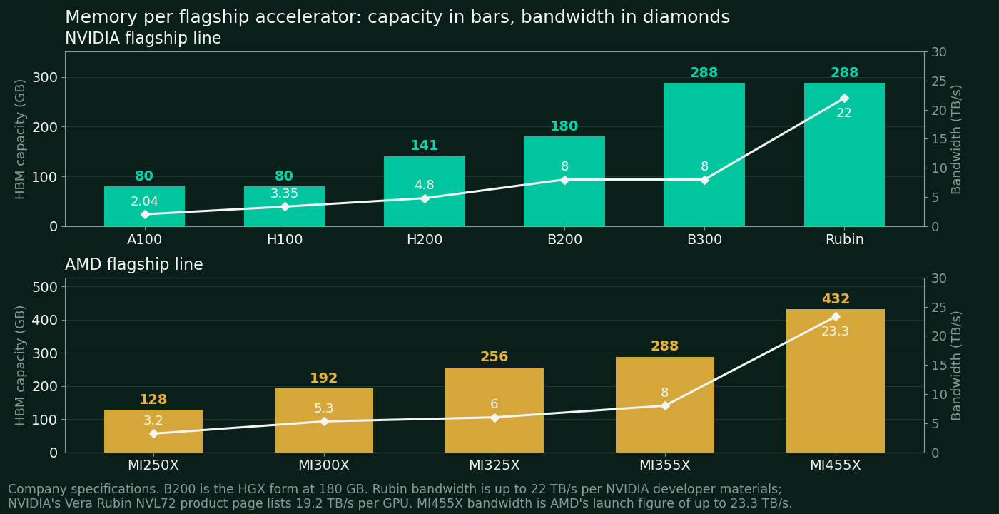
- Memory per flagship chip keeps climbing, from 80 GB on the A100 and H100 to 288 GB on the B300 and Rubin, and from 128 GB on the MI250X to 432 GB on the MI455X.
- HBM consumes roughly three times the wafer capacity of conventional DRAM per unit of output. TrendForce estimates it takes about 22% of the top three makers' wafer input at the end of 2026 to produce about 9% of the bits.
- The logic die, the HBM stacks and TSMC's CoWoS packaging must all arrive together, and TSMC chief executive C.C. Wei says packaging capacity is now limiting his customers' growth.
Because the two halves of a computer stopped growing at the same speed, and AI is the workload that exposes the gap. The warning is old. In 1995, Wulf and McKee published "Hitting the Memory Wall," arguing that processor speed was improving at about 80% a year while DRAM speed improved at about 7% a year, and that systems would eventually spend nearly all their time waiting on memory. Their paper was about latency. The AI version of the same wall is about bandwidth and capacity, and it arrived on schedule.
The cleanest modern measurement comes from Gholami and co-authors in IEEE Micro (2024). Peak server compute has grown at about 3.0 times every two years. DRAM bandwidth has grown at about 1.6 times every two years, and interconnect bandwidth at about 1.4 times. Compounded over twenty years, that is roughly 60,000 times more compute against roughly 100 times more bandwidth. The same divergence shows up inside a single vendor's line. Divide peak compute by peak bandwidth and the balance point roughly doubled in one NVIDIA generation, from about 153 FLOPS per byte on the A100 to about 295 on the H100. Each new chip needs proportionally more bytes delivered per unit of math just to stay fed.
The workload makes it worse. Training leans on large matrix multiplications that reuse data heavily. Generating text does not. In decode, the phase that produces each token, the accelerator streams the model's weights from memory with almost no reuse, so throughput is set by how fast memory can deliver bytes, not by how fast the silicon can multiply. Every token a chatbot emits is, mechanically, a full read of the model. As inference grows into the larger half of AI compute, the industry's center of gravity moves from a compute bound workload to a bandwidth bound one.
The third force is content per chip. Flagship accelerators keep swallowing more memory. NVIDIA's line went from 80 GB on the A100 and H100 to 288 GB on the B300 and the Rubin GPU. AMD's went from 128 GB on the MI250X to 432 GB on the MI455X, launched in July 2026. TrendForce puts the same shift in industry terms: HBM capacity per AI chip rose from the 96 GB and 192 GB class to the 216 GB and 288 GB class during 2026. More gigabytes per accelerator, multiplied by more accelerators, multiplies HBM bit demand even if nothing else changes.
The fourth force is that HBM eats the factory. HBM stacks are built from the same DRAM wafers as conventional memory, and a wafer committed to HBM produces far fewer bits than a wafer committed to ordinary DRAM, because the dies are larger, the yields are lower, and much of the wafer's output is consumed by stacking. The industry estimate, used by TrendForce, KB Securities, and Micron's own management, is that HBM consumes roughly three times the wafer capacity of conventional DRAM per unit of output. Treat that as an approximation, not a constant. TrendForce estimates HBM took about 18% of the top three makers' DRAM wafer input at the end of 2025 and will take about 22% at the end of 2026 and about 30% at the end of 2027, while producing only about 8%, 9%, and 13% of total DRAM bits in those years. That gap between wafer share and bit share is the whole pricing story of 2026, told in advance.
And the fifth force is packaging. An accelerator ships only when its logic die and its HBM stacks are joined on a silicon interposer in advanced packaging, TSMC's CoWoS for the NVIDIA and AMD flagships. Logic wafers, HBM stacks, and packaging slots are contracted separately, from different suppliers, on different lead times, and all three must arrive together. TrendForce estimates TSMC's CoWoS output at roughly 35,000 to 40,000 wafers a month at the end of 2024, 75,000 to 80,000 at the end of 2025, and a projected 120,000 to 140,000 by the end of 2026. On TSMC's July 2026 earnings call, chief executive C.C. Wei said packaging capacity is "so tight that now it's limiting my customers' growth," as reported in trade coverage of the call. Memory is the binding constraint of the buildout now not because DRAM is exotic, but because three constraints, wafers, stacks, and packaging, multiply each other.
How does HBM actually work?
The short version
HBM solves a wiring problem: stack the memory vertically, wire it through the silicon itself, and park it millimetres from the processor.
- A stack is DRAM core dies thinned to roughly 30 to 50 micrometres over one base die, joined by through-silicon vias and microbumps, inside a package height limit JEDEC relaxed to 775 micrometres for HBM4.
- Bandwidth is interface width times pin speed. HBM4 doubles the interface to 2,048 bits, and shipping parts run past the JEDEC 8 Gb/s baseline: Samsung at 11.7 Gb/s per pin, Micron above 11, SK hynix above 10.
- The HBM4 base die is a logic die, so the customer can design part of the stack. HBM4E has no JEDEC standard and is in customer sampling during 2026.
- Assembly splits the makers: Samsung and Micron bond with TC-NCF, SK hynix with its proprietary MR-MUF, and no maker publishes stack yields for either route.
- A flagship package needs roughly 5,000 to 25,000 data wires routed across millimetres, which only a silicon interposer can carry. Memory supply and packaging supply therefore fail or clear together.
Start with the problem it solves. A processor die can expose only so many connections along its edges. Board level memory, the DDR5 and GDDR chips on a circuit board, reaches the processor through a package substrate and a board, over distances of centimetres, at a few hundred wires. High bandwidth memory takes the opposite approach. It stacks the memory dies vertically, connects them with wires that pass through the silicon itself, and parks the stack millimetres from the processor on a shared slab of silicon. The interface is enormously wide and very short, which is how it delivers terabytes per second at a power cost a board could never match.
Each stack is a pile of thin DRAM core dies over one base die at the bottom. The core dies are ground down to tens of micrometres thick, reported at roughly 30 to 50 micrometres depending on the part and the stage, so that twelve or sixteen of them fit inside a package height limit that JEDEC held at 720 micrometres through HBM3E and relaxed to 775 micrometres for HBM4. Vertical copper filled connections called through-silicon vias, TSVs, are etched through each die and carry data, power, and control from die to die and down to the base. Tiny solder bumps, microbumps, join each die to the next. The base die holds the physical interface to the host processor, plus test, repair, and power delivery functions. It is the stack's front desk: everything the processor says to the memory passes through it.
The generations differ in three numbers: how wide the interface is, how fast each pin runs, and how tall the stack is. Bandwidth per stack is just width times pin speed. The table below keeps JEDEC standard figures separate from vendor parts, because conflating the two is the most common error in HBM tables. HBM4's headline change is the doubled interface, 2,048 bits against 1,024, set by the JEDEC JESD270-4 standard published on April 16, 2025. Shipping HBM4 parts already run well past the standard's 8 Gb/s baseline: SK hynix above 10 Gb/s per pin, Micron above 11 Gb/s with more than 2.8 TB/s per stack, and Samsung at a consistent 11.7 Gb/s and up to 3.3 TB/s per stack, all maker stated figures. HBM4E has no JEDEC standard at all. It is a vendor defined speed extension, in customer sampling during 2026, with volume production targeted for 2027.
| Generation | Interface per stack | Pin rate | Bandwidth per stack | Tallest stack | Basis |
|---|---|---|---|---|---|
| HBM2 | 1,024 bit | up to 2.4 Gb/s | up to 307 GB/s | 12 high, 24 GB | JEDEC, 2016, updated 2018 |
| HBM2e | 1,024 bit | up to 3.6 Gb/s | up to 460 GB/s | 12 high | Vendor extension; 16 GB stacks shipped in A100 and MI250X |
| HBM3 | 1,024 bit | 6.4 Gb/s | 819 GB/s | 12 high in volume | JEDEC JESD238, 2022; shipped stacks of 16 and 24 GB |
| HBM3e | 1,024 bit | about 8 to 9.6 Gb/s by bin | about 1.0 to 1.2 TB/s | 12 high in volume, 36 GB | Extension of HBM3; powers Blackwell and the MI350 series |
| HBM4 | 2,048 bit | up to 8 Gb/s per JEDEC | up to 2 TB/s per JEDEC | 16 high, 64 GB ceiling | JEDEC JESD270-4, April 2025; shipping parts exceed the pin baseline |
| HBM4E | 2,048 bit | up to 16 Gb/s target | up to about 4.1 TB/s by arithmetic | 16 high planned | No JEDEC standard; vendor samples in 2026 |
The quiet revolution inside HBM4 is the base die. Through HBM3e, the base die was a simple buffer built by the memory maker on its own DRAM process. HBM4's doubled interface and higher pin rates outran what DRAM process transistors handle well, so the base die moved to a logic process, and with that move it became designable. A customer can now put its own logic in the base die of its stacks: memory controller functions, die to die links, telemetry, even compute elements. The three makers took three different routes to the same fork.
| Maker | HBM4 core DRAM | HBM4 base die | Direction for custom and HBM4E |
|---|---|---|---|
| SK hynix | 1b nm, fifth generation 10 nm class | TSMC logic process under the April 2024 SK hynix and TSMC agreement; 12 nm class as reported | TSMC 3 nm class for custom base dies, as reported by TrendForce |
| Samsung | 1c nm, sixth generation 10 nm class | Samsung Foundry 4 nm, in house; Samsung is the only maker offering DRAM, logic, and packaging under one roof | Standard HBM4E stays in house; the reported NVHBM base die work points to TSMC 3 nm |
| Micron | 1-beta, moving to 1-gamma for HBM4E | In house advanced CMOS | Foundry base die for both custom and JEDEC HBM4E, confirmed by Micron on its September 30, 2026 call; TSMC named in trade reporting |
How the dies are joined divides the makers too. Samsung and Micron use TC-NCF, thermo compression bonding with a non conductive film, bonding one layer at a time with heat and pressure while the film becomes the underfill. SK hynix uses its proprietary MR-MUF process, introduced with HBM2E in 2019 and upgraded as Advanced MR-MUF for 12 high HBM3, in which all layers are tacked and then melted together in a single mass reflow before the gaps are filled with a molding compound. SK hynix credits the process for its thermal and warpage position on tall stacks, and it has confirmed Advanced MR-MUF for its HBM4. No maker publishes stack yields, so any precise yield comparison between the two routes is folklore and is not used here.
The expected next process step has been postponed, which is itself a fact about where the technology stands. Hybrid bonding, joining dies copper to copper with no solder bumps at all, was widely expected to become mandatory at 16 high. Instead, JEDEC's relaxation of the package height limit to 775 micrometres let 16 high stacks stay on microbumps with aggressive die thinning. SK hynix, speaking at Hot Chips in August 2026 as reported, placed its own hybrid bonding transition at HBM5 at the earliest, aimed at stacks of 20 layers and above, and Counterpoint Research projects hybrid bonding entering full scale HBM production around 2029 to 2030. Samsung is the most aggressive of the three on the technology and has demonstrated hybrid bonded work, but volume HBM through HBM4E runs on bumps.
Finally, why the stack cannot simply sit on a circuit board. One HBM3e stack presents 1,024 data pins; one HBM4 stack presents 2,048. A flagship accelerator carries five to twelve stacks, so the logic die must connect to roughly 5,000 to 25,000 data wires across a distance of millimetres. No board or ordinary substrate routes that density at that pitch. A silicon interposer, a passive slab of silicon with fine pitch wiring, sits under the logic die and the stacks and carries those wires. That is the 2.5D construction inside every flagship AI package, and it is why memory supply and packaging supply fail or clear together.
Who are the major players and who is winning?
The short version
Three companies make all the world's HBM, with one clear leader, and a fourth name, SanDisk, owns the flash tier the AI stack is learning to use.
- SK hynix leads on a qualification head start now three generations old: 63.2% of 2025 HBM revenue on IDC's figures, 50% in the second quarter of 2026 on Counterpoint's, and an estimated 60 to 70% of Vera Rubin's HBM4 volume.
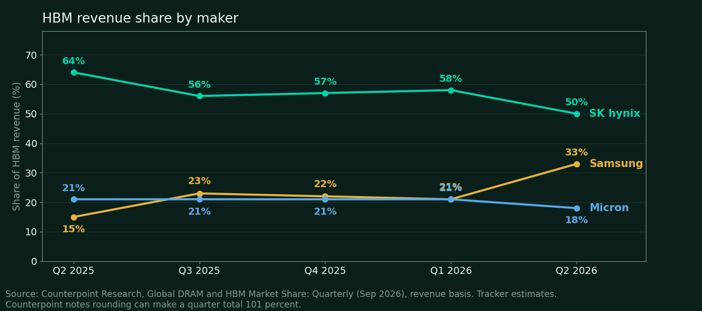
- Samsung spent about eighteen months failing NVIDIA's qualification and bottomed at 15% share in the second quarter of 2025, then recovered to 33% on its September 2025 HBM3E pass and the industry's first commercial HBM4 shipment in February 2026.
- Micron climbed from 5.8% of HBM revenue in 2024 to 17.4% in 2025, ships HBM4 in volume for Vera Rubin, has the vast majority of its 2027 HBM bits contracted at significantly higher prices, and is the only US headquartered maker.
- The bottleneck has bottlenecks: Hanmi holds about 71% of the market for the bonders that stack HBM, BESI leads hybrid bonding, and ASML's EUV systems pace every maker's next DRAM node.
- SanDisk, independent since its February 2025 separation from Western Digital, holds 11.4% of NAND revenue (TrendForce, second quarter of 2026) and, with SK hynix, sponsors High Bandwidth Flash, the attempt to give flash an HBM shaped package.
Three companies make HBM: SK hynix, Samsung, and Micron. Together they hold effectively the entire market, roughly 97% or more of HBM wafer production on the estimates cited in this article, and no fourth maker ships HBM at scale anywhere in the world. On IDC's full year figures, as charted in SK hynix's own SEC prospectus, the 2025 revenue split was SK hynix 63.2%, Samsung 19.3%, and Micron 17.4%. The quarterly view from Counterpoint Research shows what happened next: SK hynix's lead narrowed through 2026, not because it faltered, but because Samsung finally started shipping.
SK hynix built its lead the plain way: it mass produced HBM3E 12 high first, became NVIDIA's primary memory supplier through the Hopper and Blackwell cycles, and by the fourth quarter of 2024 HBM was already more than 40% of its DRAM revenue, per the company. It shipped the first 12 layer HBM4 samples to major customers in March 2025, announced HBM4 development complete with mass production ready in September 2025, began mass HBM4 shipments in the second quarter of 2026, and said in its October 28, 2026 results that HBM4 yields came in above plan and that HBM4 should pass HBM3E in both shipment and revenue share of its HBM in the fourth quarter of 2026. In June 2026 it also signed a multi year technology partnership with NVIDIA covering co design of future memory. Its position is not a share statistic. It is a qualification head start that has now lasted three generations.
Samsung's story is the opposite arc, and the most instructive in the industry. The world's largest memory maker spent roughly eighteen months failing to get its flagship part qualified at the world's largest buyer, then recovered within a year to an industry first HBM4 shipment. The timeline matters because it shows what qualification actually costs.
| Date | Samsung's HBM position |
|---|---|
| Spring 2024 | 8 high and 12 high HBM3E reportedly failed NVIDIA tests on heat dissipation and power, per Reuters and Bloomberg reporting; neither company published a failure notice |
| July 2024 | Samsung HBM3 passed NVIDIA qualification, reportedly only for the China market H20 accelerator |
| Late 2024 | 8 high HBM3E qualified for limited NVIDIA volume; the 12 high part still pending; Samsung's chairman publicly acknowledged the HBM lag |
| June 12, 2025 | AMD confirmed its MI350 series uses 288 GB of 12 high HBM3E from both Samsung and Micron, the first official confirmation of Samsung HBM3E inside a major accelerator |
| September 2025 | Samsung passed NVIDIA qualification for 12 high HBM3E, about eighteen months after the first reported failures, and began volume shipments at initially small scale |
| February 12, 2026 | Samsung announced mass production and the industry's first commercial HBM4 shipments, on 1c DRAM with a 4 nm in house base die, at 11.7 Gb/s per pin |
| March 18, 2026 | Samsung and AMD signed an agreement aligning Samsung as primary HBM4 supplier for AMD's MI455X |
| October 29, 2026 | Samsung reported HBM4 sales more than tripled quarter on quarter and reached 60% of its total HBM revenue |
The cost of the lost eighteen months is visible in the share chart: Samsung's HBM revenue share bottomed at 15% in the second quarter of 2025, a remarkable position for the largest DRAM maker on earth, and its recovery to 33% by the second quarter of 2026 came mostly from HBM3E finally shipping at scale, with HBM4 still small in first half revenue, per Counterpoint. Its recovery path from here runs through HBM4, where it shipped first, through its turnkey offer of DRAM plus foundry base die plus packaging in one company, and through AMD, where it holds the primary supplier position on the MI455X. Reported color, not company disclosure: Seoul Economic Daily put Samsung's HBM4 yield at close to 80% by August 2026, up from below 60% at the February production start.
Micron is the comeback in the other direction. IDC put Micron's HBM revenue share at just 5.8% for full year 2024. By 2025 it had reached 17.4%, and Micron said in March 2026 that it had brought its HBM share in line with its overall DRAM share during 2025. It was in volume production on 24 GB 8 high HBM3E for the H200 in February 2024, its 12 high HBM3E is designed into the GB300 platforms and dual sourced with Samsung on the MI350, and its HBM revenue reached an $8 billion annualized run rate by the quarter ended August 2025. On HBM4, Micron announced high volume production of its 36 GB 12 high part, designed for NVIDIA's Vera Rubin platform, on March 16, 2026, and cumulative HBM4 revenue above $1 billion by June 24, 2026. It is also the only US headquartered maker, with a CHIPS Act award of up to $6.165 billion and the industry's most disclosed long term agreement structure, both covered in the pricing section.
Micron's path on the quarterly series is the subtler story. It held about 21% of HBM revenue through 2025 and into the first quarter of 2026 on Counterpoint's series, then dipped to 18% in the second quarter, not on lost business but on arithmetic: Samsung's recovered volume re-entered a denominator that was itself growing fast, and Micron's own HBM revenue kept rising through the dip. Its HBM4 execution is on the record in its own releases. Volume shipments of the 36 GB 12 high part, designed for NVIDIA's Vera Rubin platform, began in the first quarter of 2026, samples of a 48 GB 16 high part followed, Micron said its HBM revenue grew faster than its total revenue in the September 2026 quarter, and by September 30, 2026 it had contracted the vast majority of its calendar 2027 HBM bits at significantly higher prices than 2026. On HBM4E it runs third rather than first: Samsung shipped HBM4E samples in May 2026 and SK hynix in June, while Micron described sampling with key customers in late 2026, on its October 21, 2026 technology webinar as relayed by BNP Paribas, with volume production targeted for calendar 2027 and the custom HBM4E implementation with NVIDIA, on a foundry made base die, as its chosen point of attack. Its capacity map is the most geographic of the three. A Singapore HBM packaging plant, about $7 billion on Reuters' figure, broke ground in January 2025 and is on track to contribute meaningfully to HBM supply in calendar 2027, per Micron's January 2026 groundbreaking release for the separate project beside it: a Singapore NAND wafer fab of about $24 billion over ten years, with wafer output scheduled for the second half of 2028. A $1.8 billion purchase of Powerchip's Tongluo fab in Taiwan closed in March 2026, per its filings, and a United States investment program above $200 billion carries the Boise and New York fabs tabled in the pricing section. The strategic fact sits underneath the map. Micron is the only maker headquartered in the country whose government is underwriting the industry, which makes it the default domestic source for US buyers and for Washington alike: the one HBM supply line that is neither Korean nor exposed to Korean politics. The alignment cuts both ways. China's Cyberspace Administration barred Micron's products from critical information infrastructure in May 2023, so the maker most aligned with US policy is also the maker with the most to lose if Beijing widens that exclusion.
On June 5, 2026, NVIDIA chief executive Jensen Huang said publicly that all three vendors had been qualified for Vera Rubin's HBM4, all were in production, and all were racing to support the platform. Qualification, though, is not allocation. Supply chain estimates for the Vera Rubin HBM4 volume split put SK hynix at roughly 60 to 70%, Samsung at roughly 25 to 30%, and Micron at the remainder. Those are estimates from UBS and other trackers, not NVIDIA disclosures, and they describe the market's real hierarchy better than the qualified list does: three suppliers, one clear first among them.
Beneath the three makers sits an equipment and materials layer that the shortage has made valuable. Hanmi Semiconductor holds about 71% of the global market for the thermo compression bonders that stack HBM dies, per TechInsights data cited in February 2026, with ASMPT taking share inside SK hynix's HBM4 fleet and Samsung's captive SEMES supplying most of Samsung's own line. BESI leads die to wafer hybrid bonding with an estimated two thirds share, and Applied Materials owns about 9% of BESI and sells a joint hybrid bonding system with it. SK hynix's MR-MUF process depends on a molding resin co developed with Japan's Namics over roughly fifty iterations, with Namics as the exclusive qualified supplier and sector reporting putting the exclusivity's expiry near early 2027. Test is concentrated as well, between Advantest and Teradyne. And at the front end, ASML's EUV systems pace the advanced DRAM nodes all three makers are migrating to, with ASML's chief executive saying on October 14, 2026 that planned EUV and immersion capacity rises about 30% in 2027 and another 30% in 2028. The share figures in this paragraph rest largely on single research compilations and are directional, but the structure is not in doubt: the bottleneck has bottlenecks.
SanDisk: the champion of the tier below. One more company belongs in this section even though it makes no DRAM and no HBM at all. SanDisk is the only large pure play NAND maker headquartered in the United States, independent since it completed its separation from Western Digital on February 21, 2025 and listed on Nasdaq under SNDK. On TrendForce's second quarter 2026 ranking it stands fifth in NAND revenue at $8.97 billion and 11.4%, behind Samsung at 29.3%, the SK hynix group including Solidigm at 18.2%, Micron at 15.1%, and its own manufacturing partner Kioxia at 13.6%. It owns no wafer fab. Substantially all of its flash comes from Flash Ventures, the joint venture entities it holds at 49.9% alongside Kioxia, whose Yokkaichi and Kitakami plants in Japan make the wafers both companies sell under their own brands. The partners extended that framework in January 2026 through December 2034, and on August 27, 2026 announced anticipated investment of more than $31 billion in the two plants through 2032, contingent on Japanese government support. Its volume silicon is BiCS8 at 218 layers, co developed with Kioxia. Its next generation, BiCS10 at 332 layers in a 1 terabit TLC die, began sampling in July 2026, is about 59% denser than BiCS8 on the partners' published figures, and is expected in mass production in 2027 at Kitakami.
What pulls a flash maker into an AI memory article is the demand arriving underneath the accelerator. Training clusters stream datasets and write checkpoints to enterprise SSDs, and inference increasingly parks its state there too: NVIDIA's ICMS tier, covered in the buyers section, is a pod level flash cache built from drives of exactly this class, and Citi estimates it alone puts about 1,152 TB of SSD NAND into each Vera Rubin system. SanDisk's reported numbers show the pull directly. Its datacenter revenue rose 437% in fiscal 2026, a year in which total revenue rose 175% to $20.25 billion, and TrendForce recorded its data center business growing more than 200% quarter on quarter in the first quarter of 2026 alone. It has also adopted the contract structure of the tiers above it: five long term New Business Model agreements announced during its April 2026 earnings call and five more signed by August, converting flash bits into multi year commitments in the same season the DRAM makers were doing the same with theirs. Its second quarter revenue growth of 50.7% was the slowest of the five NAND makers, and TrendForce attributed the pace to conservative bit shipment growth: in a shortage, SanDisk is selling certainty rather than spot upside. Its route into the package itself is High Bandwidth Flash, the standard it originated in February 2025 and now develops with SK hynix, covered in the buyers section. Until HBF ships, SanDisk's position is the mirror of the HBM makers': no part inside the accelerator, and an increasingly contracted claim on everything the accelerator needs to remember between computations.
What does the ground say about pricing and capacity?
The short version
Conventional memory repriced violently, HBM repriced on a lag, and the deepest change is contractual: supply is now sold years ahead with buyers' cash down.
- Conventional DRAM contract prices compounded to roughly five times their year earlier level by the third quarter of 2026 on TrendForce's published ranges, and NAND followed the same wafer migration upward.
- 2026 HBM prices actually declined for the incumbent supplier base under annual agreements set the year before, and server DDR5 briefly earned more per wafer than HBM. The 2027 round reversed the order, with TrendForce forecasting blended HBM prices up 121%, mix shift included.
- 2026 HBM supply sold out at all three makers, and by late October 2026 all three said their 2027 HBM volumes were negotiated or contracted at higher prices.
- Long term agreements are the new structure: Micron counts 26 strategic agreements backed by about $32 billion of customer commitments, SK hynix has agreements with 14 customers covering more than half of its 2027 and 2028 capacity, and Samsung aims to place 60 to 70% of its medium term capacity under contract.
- Relief sorts by year: line conversions, the M15X ramp and packaging additions are the 2027 valve, while the new fabs produce from 2028 onward. The makers guide to tight supply through 2028 (Samsung), through 2030 (SK hynix), and tighter in 2027 and 2028 than in 2026 (Micron).
It says the shortage repriced everything except, for one strange year, HBM itself.
Conventional DRAM is priced in quarterly contracts, and TrendForce's published ranges describe the steepest sustained rise in the industry's history: up 45 to 50% in the fourth quarter of 2025, up 93 to 98% in the first quarter of 2026, up 58 to 63% in the second, up 13 to 18% in the third, with a further 10 to 15% forecast for the fourth. Compounded, contract prices in the third quarter of 2026 stood at roughly five times their level of a year earlier. This is the wafer math of the first section arriving as an invoice: every wafer that moved into HBM was a wafer removed from a conventional market that had no spare capacity of its own. NAND followed the same direction on the same mechanism, up 55 to 60% in the first quarter of 2026 and 70 to 75% in the second on TrendForce's ranges, as makers protected margins and AI storage demand, including NVIDIA's new flash cache tier covered below, pulled bits upward.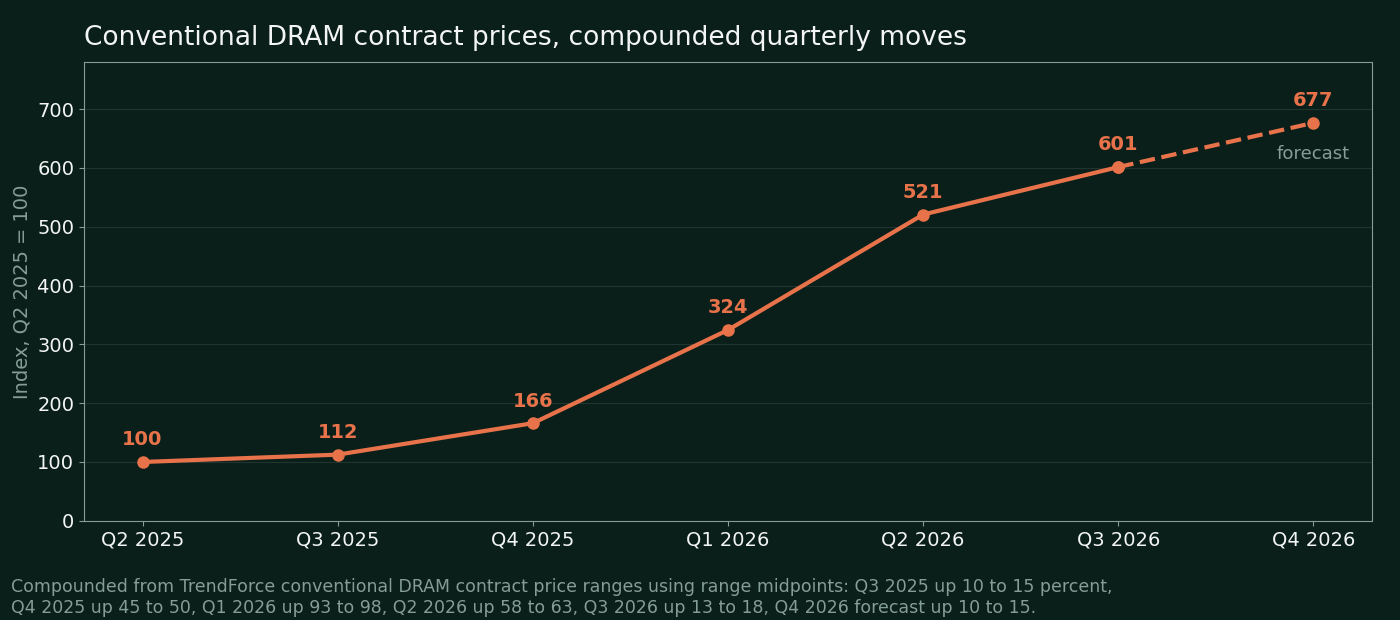
HBM pricing ran the other way in 2026, for a contractual reason. HBM is priced on annual agreements set the year before, so while conventional DRAM repriced violently quarter by quarter, 2026 HBM contract prices for the incumbent supplier base actually declined, on TrendForce's account, and SK hynix's average selling price growth in early 2026 was partly constrained by exactly that. By the first quarter of 2026, TrendForce's per wafer revenue analysis had DDR5 64 GB server RDIMMs earning more per wafer than HBM, and Samsung's chief financial officer said in May 2026 that server DDR5 profitability had overtaken HBM3E profitability for the first time. The makers entered the 2027 negotiations, which TrendForce described in June 2026 as stalled over price, determined to reverse that. By late October 2026 the talks had largely landed: SK hynix said 2027 HBM volume and pricing with major customers were already negotiated, Samsung said its 2027 HBM supply was fully sold at target prices, and Micron said the vast majority of its calendar 2027 HBM bits were contracted at significantly higher prices than 2026. TrendForce forecasts blended HBM average prices up 121% in 2027, a figure that includes the mix shift toward higher priced HBM4 and is not a like for like rise on the same part. Tracker estimates, not contract disclosures, put HBM3 at about $200 per stack, HBM3E at about $300, and HBM4 36 GB at about $500 to $550. Fubon Research estimated HBM4 at $31 to $32 per gigabyte for NVIDIA and $35 to $36 for other buyers, against $17 to $18 for HBM3E.
The sold out chronology is worth stating plainly, because it is the demand side of every price above. Micron said on December 17, 2025 that it had completed agreements on price and volume for its entire calendar 2026 HBM supply, including HBM4. Samsung's 2026 supply was reported sold out by October 2025, after its NVIDIA qualification pass. TrendForce's bulletin of November 4, 2026 summarized the position in one line: HBM4 is ramping, and next year's supply is sold out. The HBM market was worth about $35 billion in 2025 on Micron's and Yole's figures, and specialist estimates for 2026 cluster in a $45 to $60 billion band. The wider DRAM industry's revenue tells the scale of the repricing: $53.58 billion in the fourth quarter of 2025, $97.0 billion in the first quarter of 2026, and $154.73 billion in the second, all TrendForce figures. The profit followed the same curve. SK hynix posted an 80% operating margin in the third quarter of 2026, Samsung's chip division earned about 99% of group operating profit, and Micron's fiscal 2026 revenue of $133.19 billion was three and a half times its fiscal 2025 revenue of $37.38 billion.
The long term agreement era
The structural change underneath the prices is contractual. Memory used to be bought quarter to quarter. It is now bought half a decade at a time, with the buyers' cash on the makers' balance sheets. Micron disclosed 26 strategic customer agreements by September 30, 2026, most running about five years, backed by about $32 billion in customer financial commitments, the vast majority as upfront cash deposits. Its customer contract liabilities rose to $12.9 billion from $568 million in May 2026. The agreements are take or pay, and about three quarters of their estimated revenue carries price floors and ceilings. Micron expects them to cover more than 35% of revenue through 2030, and says more than 75% of its calendar 2027 output was already committed. SK hynix said on October 28, 2026 that it had signed long term agreements with 14 major customers covering more than 50% of its total production capacity for 2027 and 2028, on typical terms of about five years, and management said that agreements plus volumes under concrete negotiation leave its DRAM and HBM capacity effectively sold out through 2029. Samsung said on October 29, 2026 that it had multi year agreements with 10 major customers and 10 more in negotiation, with a goal of placing 60 to 70% of its medium to long term capacity under such contracts. Korean industry reporting summarized by Hankyung on November 2, 2026 puts five year base terms and deposits of 20 to 25%, or take or pay terms, as the new industry default. One number to read carefully: OpenAI's letters of intent with Samsung and SK hynix of October 1, 2025 attach to a projected demand of up to 900,000 DRAM wafers a month. That is OpenAI's stated appetite, not an order, and as of November 2, 2026 reporting it remained unclear whether the letters had converted into firm orders.
Capacity is where the ground contradicts the headlines. Announced investment figures are enormous, but wafers arrive on a fab's schedule, not a press release's. Samsung told investors that more than three and a half years elapse between starting a new fab and producing wafers from it. Sorted by when output can actually ship, the buildout divides cleanly into relief that exists in 2027 and relief that does not.
| Project | Maker | What it adds | When it produces |
|---|---|---|---|
| M15X, Cheongju | SK hynix | HBM4 front end fab, ramping to maximum HBM4 capacity by end of 2026 | 2026 into 2027; the one real near term valve |
| P4 line conversions, Pyeongtaek | Samsung | Existing lines converted to the 1c process, above 200,000 wafers a month of 1c capacity targeted by end of 2026 | 2026 into 2027 |
| Packaging additions, Taiwan and Singapore | Micron | Taichung AATT2 packaging plant opened October 16, 2026; Singapore HBM packaging output from early 2027 | 2027, back end only |
| Yongin cluster, first fab | SK hynix | First fab of a four fab cluster; cleanroom opening moved up to February 2027 | Cleanroom is not production; volume late 2027 into 2028 |
| Boise ID1, Idaho | Micron | First new US leading edge DRAM fab; first wafer output targeted mid 2027, about two years behind its original 2022 schedule | Ramp late 2027 into 2028 |
| Pyeongtaek P5 | Samsung | New fab, planned as an HBM hub | Mass production targeted for the latter part of 2028 |
| P&T7, Cheongju | SK hynix | Advanced packaging and test hub paired with M15X, completing end of 2027 | Output contribution 2028 |
| Boise ID2, Idaho | Micron | Second Boise fab | First wafers targeted late 2028 |
| West Lafayette, Indiana | SK hynix | Advanced packaging and R&D, investment restated above $4 billion at the August 2026 groundbreaking; wafers still fabricated in Korea | Mass production moved to the second half of 2029, slipped from 2028 in the original 2024 plan |
| Clay, New York | Micron | Four fab megasite, groundbreaking January 2026 | First fab operation about 2030 on the final environmental timeline |
Public money follows the same slow clock. Under the CHIPS Act, Micron's award is up to $6.165 billion, Samsung's is up to $4.745 billion for its Texas logic complex, which makes no memory, and SK hynix's is up to $458 million plus up to $500 million in loans for Indiana. The makers' own outlooks agree with the table rather than with the investment headlines: SK hynix expects demand to exceed supply through 2030, Samsung expects tight supply through 2028, and Micron expects calendar 2027 and 2028 to be tighter than 2026, with industry DRAM bit supply growing only in the low twenty percent range in both years. TrendForce's summary of the mechanism is that 2026 to 2027 bit growth comes mainly from process migration, not new wafer starts. In plain terms: 2027 relief is conversions, packaging, and better nodes. The new buildings are a 2028 and later story.
What are the buyers doing about it?
The short version
No buyer can make DRAM, so they redesign the one layer that became designable, route work to cheaper memory tiers, and buy supply years ahead.
- Custom base dies are real but early. Marvell announced the first custom HBM architecture in December 2024; NVIDIA's NVHBM claims up to 30% more bandwidth against a standard that was not yet shipping, with Amazon's Annapurna as a collaborator rather than a disclosed customer; and Broadcom has no base die answer (Counterpoint).
- Substitution starts with LPDDR. SOCAMM2 modules ship with the Vera CPU at up to 1.5 TB per CPU, yet TrendForce estimates the makers' 2027 LPDDR output covers only about 60% of NVIDIA's requirement.
- Flash is the next tier down. NVIDIA's ICMS holds key value cache in flash at pod level, a tier Citi estimates at about 9.3% of global NAND demand in 2027, while High Bandwidth Flash remains years from silicon anyone can buy.
- The third lane is the contract itself: multi year take or pay agreements and deposits in the tens of billions, because customization redistributes design margin and moves not a single DRAM wafer.
- TrendForce's second quarter 2026 DRAM revenue ranking, Samsung 39.4%, SK hynix 24.9%, Micron 23.3%, CXMT 9.5%, contains no cloud company and no chip designer at any rank.
Every large buyer of AI memory has reached the same conclusion from a different direction: they cannot make DRAM, and they cannot wait for the market to clear. What they can do falls into three lanes. They can redesign the part of the stack that is now designable. They can route some workloads to cheaper memory tiers. And they can lock in supply with contracts and cash. The lanes are worth separating, because they have very different states of reality.
Lane one: custom base dies. The HBM4 base die's move to a logic process opened a door, and the first named design through it was not NVIDIA's. On December 10, 2024, Marvell announced a custom HBM compute architecture that moves HBM support logic onto the base die, claiming up to 70% lower interface power, up to 25% of the accelerator die area freed, and support for up to 33% more stacks per accelerator, with Micron, Samsung, and SK hynix named as collaborators. NVIDIA arrived twenty months later with the bigger platform. On August 26, 2026 it announced NVHBM under its NVLink Fusion program: NVIDIA's custom memory controller moves into the HBM base die, with claimed gains, all stated as up to figures and all measured against an HBM4E standard that was not yet shipping, of 30% more bandwidth, 15% lower HBM power, and 25% more area freed on the compute die. NVIDIA says it is establishing a standard NVHBM implementation available from multiple memory providers, and named none of them. Amazon's Annapurna Labs will be the first to work on NVHBM, tied to Trainium4 through NVLink Fusion. Read that wording precisely: a collaborator on a platform offer, not a disclosed purchase order, with no ship date, and the Vera Rubin systems already shipping use standard HBM. A reported layer sits on top: Seoul Economic Daily reported on October 18, 2026, relayed by Reuters, that NVIDIA had asked all three makers to build NVHBM base dies on TSMC's 3 nm process and that Samsung had accepted. No company has confirmed it. The partial corroboration is Micron's: on its September 30, 2026 call, Micron confirmed that the HBM4E base die, for both the custom NVHBM product and the JEDEC product, moves to a foundry process, where its HBM4 base die was made in house. And the dog that has not barked is Broadcom, the largest custom silicon designer of all. Counterpoint Research's August 31, 2026 analysis states it directly: Broadcom has no base die answer. Its verified offer is packaging, a 3.5D platform carrying up to twelve HBM stacks. How much of HBM4 demand ends up custom is genuinely unknown: the available proxies conflict, with analyst estimates putting HBM4E at anywhere from 9% of 2027 HBM demand (UBS, October 2026) to about 40% (analysts cited by Chosun Biz in November 2025), and the custom share inside HBM4E is disclosed by nobody.
Lane two: substitution tiers. The cheapest gigabyte is the one that never had to be HBM, and the industry is building a staircase of slower, larger tiers below the stack. The first step is LPDDR5X on modules. NVIDIA's SOCAMM module, a socketed, serviceable LPDDR module developed with the three makers, was built for the CPU side of its racks. Its first generation reportedly failed on the GB300 platform on thermal grounds, per trade reporting that NVIDIA has not confirmed, and GB300 shipped with soldered LPDDR5X instead. The standardized second generation, JEDEC's JESD328 SOCAMM2 of October 2025, runs LPDDR5X at up to 9.6 Gb/s per pin and ships with the Vera CPU in the Vera Rubin platform: up to 1.5 TB of LPDDR5X per CPU at 192 GB modules, roughly 54 TB per rack. Even this tier is short. SemiAnalysis reported on June 4, 2026 that most Vera Rubin racks would ship with 96 GB modules, about 768 GB per CPU and roughly 28 TB per rack, because LPDDR5X itself is scarce; the sockets at least make the missing capacity upgradeable later. TrendForce estimates the three makers' combined 2027 LPDDR output covers only about 60% of NVIDIA's requirement, and one reported price index had 12 GB LPDDR5X contract pricing up 89% in a single quarter of 2026. Supply is real at this tier: SK hynix put a 192 GB SOCAMM2 into mass production on April 19, 2026, and Micron shipped samples of a 256 GB module in March 2026, the largest LPDRAM module it has offered, enabling up to 2 TB per CPU.
The second step down is flash pretending to be memory. High Bandwidth Flash, HBF, stacks NAND dies in an HBM like package to trade speed for capacity. SanDisk originated it in February 2025, SK hynix joined as standards partner that August, and the effort lives in the Open Compute Project, not JEDEC: the consortium launched on February 25, 2026, and the first standard specification arrived on August 4, 2026, with capacity up to 512 GB per stack in 8 and 16 high configurations, three bandwidth grades from about 0.4 to 3.0 TB/s, and a UCIe connection to the processor. Google and Tenstorrent are named consortium participants, and Meta was reported joining in August 2026. None of them has been announced as a buyer, and no accelerator design win has been disclosed. The timing has also slipped on the sponsors' own documents: the August 2025 agreement targeted first samples in the second half of 2026 and inference device samples in early 2027, while SanDisk said at its August 2026 investor day that customer samples would come next year, and SK hynix's own timeline at the August 2026 specification launch put the full specification in early 2027 and first samples in early 2028. The consortium's own launch material expects demand for composite memory designs including HBF to take off around 2030. HBF is a real standard with a real capacity argument, 512 GB against HBM4's 36 GB volume stacks, and it is years from silicon anyone can buy.
NVIDIA's own version of the flash tier is already a product. The Vera Rubin platform includes ICMS, Inference Context Memory Storage, an Ethernet attached flash layer powered by its BlueField 4 processor that holds key value cache at pod level, sized in petabytes, positioned between the GPU's memory and durable storage. NVIDIA claims up to five times the tokens per second and five times the power efficiency of traditional storage approaches for that role, with the baseline undisclosed. Citi estimates the tier adds about 1,152 TB of SSD NAND per Vera Rubin system and takes ICMS driven NAND demand to about 9.3% of global NAND demand in 2027. That is one analyst's estimate, but the direction is the point: the substitution lanes relieve HBM at the margin while adding demand to every other memory tier.
Lane three: lock in, because nobody is fabbing DRAM. The deepest fact in this article is a negative. No hyperscaler and no accelerator designer fabricates DRAM. TrendForce's second quarter 2026 DRAM revenue ranking reads Samsung 39.4%, SK hynix 24.9%, Micron 23.3%, and CXMT 9.5%, and no cloud company or chip designer appears on the maker side of it at any rank. NVIDIA designs the NVHBM base die and does not make it; a foundry does, and the DRAM dies on top of it still come from the same three companies. Customization redistributes design work and margin. It does not move a single DRAM wafer. So the buyers' third lane is the contract structure already described: multi year take or pay agreements, deposits in the tens of billions, and capacity spoken for years ahead. The memory makers have become, in effect, utilities with a three firm supply side, and the largest technology companies on earth are queuing for allocations like it.
How is China catching up?
The short version
China has already caught up in NAND, is a genuine fourth force in conventional DRAM, and remains about two HBM generations behind a wall built of equipment and import controls. The dated verdict by layer is at the end of this section.
- The December 2024 US rule captures every HBM stack in production, Korean made included, through its bandwidth density threshold and Foreign Direct Product provisions, and controls 24 types of chipmaking equipment in the same package.
- China stockpiled ahead of the deadline. SemiAnalysis estimates about 13 million HBM stacks arrived in total, enough for roughly 1.6 million Ascend class packages, and Epoch AI models the stockpile as fully spent during 2026.
- Huawei's ceiling is memory, not logic. Its answer is proprietary memory, HiBL 1.0 and HiZQ 2.0, the latter stated at 144 GB and 4 TB/s for the Ascend 950DT, with the manufacturer undisclosed.
- CXMT holds 9.5% of global DRAM revenue (TrendForce) with capacity heading toward about 350,000 wafer starts a month, but its DDR5 density matches what the leaders shipped in 2021, its listing prospectus contains no HBM, and its HBM3E samples yield 20 to 30% against about 70% at SK hynix (Reuters).
- YMTC is the counterexample: 16.5% of global NAND shipments, 267 layer NAND in mass production, a 294 layer part shipped, and Samsung licensing its hybrid bonding patents. In NAND, China is at the frontier.
China's memory story splits cleanly in two, and blending the halves is the standard error. In conventional DRAM and in NAND, China has real, shipping, globally competitive supply. In HBM, the product this article is about, it has samples, plans, and a stockpile. Start with the wall China built against itself being necessary at all: the controls. On December 2, 2024, the US Bureau of Industry and Security issued a rule creating ECCN 3A090.c, controlling HBM with a memory bandwidth density above 2 GB/s per square millimetre. BIS stated that all HBM stacks in production exceed that threshold, which means HBM2, HBM3, and HBM3E are all captured with no generational carve out, and the rule's Foreign Direct Product provisions reach HBM made outside the United States, including Korean made stacks, when it is a direct product of US technology. The compliance date was December 31, 2024. The same package controlled 24 types of semiconductor manufacturing equipment and added roughly 140 entities to the Entity List.
Everyone involved saw the date coming, and the stockpiling that preceded it is the best evidence of how binding the constraint is. SemiAnalysis estimates that Samsung alone directly provided about 11.4 million HBM stacks to China, including about 7 million in the single month between the rule's announcement and its compliance date, and about 13 million stacks in total across providers and routes. At eight stacks per accelerator package, that is roughly 1.6 million Ascend class packages. Epoch AI models the stockpile as fully spent during 2026. Teardown evidence supports the arrangement: TechInsights found TSMC made logic dies and Samsung and SK hynix HBM inside Huawei's Ascend 910C. The flow since the controls is contested reporting rather than established fact: The Information reported on November 2, 2026 that Huawei has told some clients a large share of its upcoming Ascend 960DT will run largely on Samsung and SK hynix HBM, and that smuggled HBM3E trades on China's grey market at about $4,000 per unit. Both are single source reports and are labeled as such here.
Huawei's position is that memory, not logic, is its ceiling. The 910C pairs two dies built on SMIC's N+2 process, a 7 nm class DUV process without EUV, with yields reported from about 20% for the 910C to about 50% for the earlier 910B, against the 70% plus that volume economics usually need. Every serious outside analysis, from SemiAnalysis, Epoch AI, and others, reaches the same conclusion: SMIC could stamp more logic dies than Huawei can feed with HBM. Huawei's answer, laid out by rotating chairman Eric Xu at Huawei Connect on September 18, 2025, is a proprietary memory line of its own. The Ascend 950PR, for prefill and recommendation workloads, was slated for the first quarter of 2026 on HiBL 1.0, a proprietary memory Huawei described only as more cost effective than HBM3E and HBM4E, with no capacity or bandwidth figure given. The 950DT, for decode and training, was slated for the fourth quarter of 2026 on HiZQ 2.0 at a stated 144 GB and 4 TB/s. The 960, due in the fourth quarter of 2027, doubles the 950's compute, memory bandwidth, and memory capacity, and the 970 follows in the fourth quarter of 2028. Who manufactures HiBL and HiZQ, on what node, at what yield and volume, Huawei did not say. Treat the 950 dates as Huawei's plans: outside sources do not confirm the 950PR shipped on schedule, and Reuters reported in March 2026 a base 950PR card on conventional DDR beside a premium HBM version, which sits awkwardly with the keynote framing.
CXMT, China's DRAM champion, is simultaneously bigger than the headlines suggest and further behind where it counts. In conventional DRAM it is a genuine fourth force: 9.5% of global DRAM revenue in the second quarter of 2026 on TrendForce's count, estimated capacity of roughly 265,000 to 300,000 wafer starts a month heading toward about 350,000 by the end of 2026, against Micron's estimated 375,000 to 385,000. Its DDR5 ships inside Lenovo laptops and has passed server validation at Tencent and ByteDance on reporting around its July 2026 Shanghai listing. The technology gap shows in the silicon: its mainstream DDR5 sits on a roughly 16 nm class node, TechInsights teardown analysis puts its chip density at about the level the leaders shipped in 2021, and its DDR5 die is roughly 40% larger than Samsung's equivalent per Trefis, which means fewer chips per wafer and a structurally worse cost base. In HBM, the hardest fact is a disclosure by omission. CXMT's May 2026 listing prospectus, a document that funds 29.5 billion yuan of projects, contains no HBM product and no HBM project. CXMT has no HBM on sale. What exists, on the best reporting, is sampling: HBM3 samples to Huawei and other domestic designers since the second half of 2025 at pilot volumes, with SemiAnalysis estimating yields near 25% on 8 high parts, and, per Reuters on October 28, 2026 citing people familiar with the matter, HBM3E samples shipped to several Chinese AI chip designers with limited production planned within two months at yields of only 20 to 30%, against roughly 70% at SK hynix, and test performance closer to HBM3 than to HBM3E. CXMT did not confirm the report. Set against SK hynix shipping HBM4 in volume and sampling HBM4E, the honest assessment is two full product generations of gap plus roughly forty points of yield, which analysts variously translate into three to four years. The gap is specific, not general: it lives in TSV stacking, base die integration, and advanced packaging, compounded by no access to EUV.
YMTC is the counterexample that proves the specificity. China's NAND maker, on the US Entity List since December 2022, held 16.5% of global NAND shipments in the second quarter of 2026 on Counterpoint's count, third in the world, and 14% of bit shipments. It mass produces 267 layer NAND, has shipped a 294 layer part on its Xtacking 4.0 architecture with TechInsights confirming the structure and its wafer to wafer hybrid bonding at above 90% array efficiency, and Samsung licensed YMTC's hybrid bonding patents in early 2025 for its own 400 layer generation. In NAND, China is not catching up. It is, in one measurable dimension, ahead. The wall is around stacked DRAM specifically, and it is holding for now.
The verdict: when does China catch up?
NAND: it already has, on the axis the industry races on. YMTC ships layer counts at the frontier and holds the lead in wafer to wafer hybrid bonding, the technique Samsung licensed from it in early 2025. What China lacks in NAND is not technology but sanctioned scale: at 16.5% of global shipments YMTC is the world's third supplier, and every additional fab it equips must be equipped under export controls. Technology parity in NAND is a present fact, dated 2025 to 2026. Share parity has no evidence based date, because it depends on equipment access rather than on anything YMTC has left to invent.
Conventional DRAM: a volume force now, a price force through the late 2020s, node parity not datable. CXMT approaches Micron's wafer scale by the end of 2026 and already forces price competition in the commodity segments it can ship. But its shipping density matches the level the leaders shipped in 2021, a lag of roughly five years that EUV denial freezes in place: the leaders keep moving, and the gap closes only if Chinese lithography reaches production grade, an event no source in this record can date. The honest verdict is two verdicts. In the market sense, catch up is happening now and caps commodity DRAM prices through the late 2020s. In the technology sense, cost per bit parity at the frontier node has no evidence based date while EUV stays denied.
HBM: domestic supply becomes real in 2027, frontier parity not before 2029. The arithmetic is this section's own. CXMT's HBM3E samples test closer to HBM3, at yields of 20 to 30% against roughly 70% at SK hynix, with limited production planned from late 2026. That supports genuine, low volume, domestically consumed HBM3 class supply during 2027, the first year after Epoch AI's modelled stockpile runs out. Two product generations plus roughly forty points of yield is what analysts translate into three to four years, which from late 2026 puts frontier parity, HBM4 class parts at competitive yields, in 2029 to 2030 at the earliest. Three things could move that earlier: indigenous etch, deposition and bonding tools qualifying faster than expected; grey market HBM flows persisting at scale; or Huawei's proprietary HiBL and HiZQ parts delivering their stated specifications on schedule, which would let Huawei route around the JEDEC ladder for its own accelerators without CXMT matching the leaders. Tighter enforcement, or CXMT yields stalling in the twenties, moves it later. And one piece of the question cannot be dated at all: the manufacturer, process node and yield behind HiBL and HiZQ, because Huawei has disclosed none of them. Any verdict that pretends otherwise is inventing precision.
How does the memory play evolve as AI itself changes?
The short version
Inference rewrites the demand side: the cache a model must remember grows with every token, every user and every agent loop, faster than the mitigations shrink it.
- The key value cache grows linearly with context length and simultaneous users. A small 8B model needs 17.2 GB of cache at a 128,000 token context, more than three times the size of its own 4 bit weight file.
- The mitigations bend the curve without reversing it: grouped query attention, sliding window layers, and cache quantization, which takes the cache to about 29% of its 16 bit size at 4 bit.
- Agentic systems run at 5 to 30 times the tokens per task of a chatbot interaction (Gartner, as cited), and inference is roughly two thirds of AI compute demand in 2026, heading toward about 75% by 2030 on industry estimates.
- Per chip content keeps rising, 288 GB of HBM4 on Rubin and 432 GB on the MI455X, while supply bends even flagship designs: Rubin Ultra's announced 16 stack, roughly 1 TB configuration is reported redesigned to 8 stacks and about 384 GB, unconfirmed by NVIDIA.
- On relief timing the sources split: Gartner sees the earliest broad relief in late 2027, Bernstein a possible industry peak in the second half of 2027, and the makers describe no relief this side of the 2028 fab wave.
The demand side of the play is being rewritten by what a query now contains.
A language model serving a conversation must remember the conversation, and the memory it uses is the key value cache: the stored keys and values of every token already processed, which the model rereads to produce each next token. The cache's size is mechanical: two, for keys and values, times batch size, times sequence length, times layers, times attention heads, times head dimension, times bytes per element. It grows linearly with context length and with the number of simultaneous users, and at modern context lengths it dwarfs the model itself. A Llama 3.1 8B, a small model with grouped query attention, needs 128 KiB of cache per token: 17.2 GB at a 128,000 token context, more than three times the size of its own 4 bit weight file at 4.9 GB. A 70 billion parameter model with full multi head attention needs about 2.6 MB per token, about 335 GB of cache at 128,000 tokens, which is an upper bound that modern attention designs exist specifically to avoid. The mitigations are real and they bend the curve: grouped query attention, sliding window layers, and cache quantization, which takes the cache to about 54% of its 16 bit size at 8 bit and about 29% at 4 bit. Any demand model that ignores the mitigations overstates memory per token for new models. Any model that ignores context growth understates it. The two forces fight, and so far context and concurrency are winning.Agentic workloads multiply the same arithmetic. An agent does not ask one question; it loops, and on every step its framework resends the accumulated context, the system prompt, the tool definitions, the history, and the tool outputs. Gartner, as cited in practitioner material through 2026, puts agentic systems at 5 to 30 times the tokens per task of a standard chatbot interaction. Reasoning models stretch it further from the other side, generating thousands of thinking tokens per query, each one extending the cache. This is why the workload mix matters as much as the chip mix: industry estimates put inference at roughly two thirds of AI compute demand in 2026, with analysts predicting roughly 75% by 2030, and inference is the bandwidth and capacity bound half of the business. NVIDIA's own platform design concedes the point: its ICMS flash tier exists, in NVIDIA's framing, because inference state in the agentic era routinely outlives a single GPU's execution window and the cache becomes a shared pod level resource. When the company selling the accelerators builds a product whose job is to hold memory the accelerator cannot, the memory play has become the main play.
Per chip, the ladder continues. Rubin carries 288 GB of HBM4; AMD's MI455X carries 432 GB across 12 stacks; the custom silicon follows the same slope, with Google's Ironwood at 192 GB of HBM3E, Microsoft's Maia 200 at 216 GB, Amazon's Trainium3 at 144 GB, and Maia 300 reported at 288 GB of HBM4. A single reported illustration scales it: Hankyung reported in November 2026 that a 100 MW hyperscale AI data centre typically holds about 40,000 NVIDIA GPUs needing about 330,000 HBM stacks. SK hynix expects HBM4 to pass HBM3E in its HBM mix during the fourth quarter of 2026, while analyst consensus still has HBM3E at roughly two thirds of 2026 HBM shipments. HBM4E then becomes the 2027 ramp question, against Rubin class and MI400 class platforms, and the honest state of its flagship application is unsettled in a way that summarizes the whole era. NVIDIA announced Rubin Ultra for the second half of 2027 with 16 HBM4E stacks and about 1 TB of memory per package. SemiAnalysis reported on June 30, 2026 that the four die package behind that design had been cancelled because TSMC's CoWoS-L packaging hit its limits at that interposer scale, and that the shipping part would carry 8 stacks and about 384 GB. TrendForce's demand models use 384 GB per GPU for Rubin Ultra in 2027, and TrendForce reported in August 2026 that NVIDIA was weighing still lower memory configurations, 8 high HBM4E, 12 high HBM4, and 8 high HBM4, under DRAM supply pressure. NVIDIA has not publicly confirmed a redesign. Even the largest chip designer's flagship is being specified by packaging limits and memory supply rather than by its own architects.
Supply pressure is now visibly bending product configurations in smaller ways too. TrendForce reported in October 2026 that HBM stacks are converging toward lower layer counts, with 8 high expected to become mainstream in the second half of 2027 and 16 high volume pushed later, and it estimates 8 high HBM will cost 10 to 20% more per gigabit than 12 high in 2027, because the expensive logic base die is spread across fewer DRAM dies. The base die, a component that did not exist as a commercial battleground three years ago, now sets stack heights. What the 2027 to 2028 supply path does to pricing power is the one question every source answers differently. Gartner's February 2026 view had combined DRAM and SSD prices rising about 130% across 2026 with the earliest broad relief in late 2027. Bernstein is the closest named caution, seeing price rises slow after the second quarter of 2026 and a possible industry peak in the second half of 2027. UBS models the supply demand gap widening into 2027. And the makers themselves, SK hynix through 2030, Samsung through 2028, Micron tighter in 2027 and 2028 than in 2026, describe no relief at all this side of the new fabs. The spread between those views is the investment question, and the fab table above is the arbiter: on announced capacity, the physical relief is a 2028 event.
What would break the memory trade?
The short version
Memory breaks the way it always has, through inventory, digestion and a capacity wave arriving after demand slows. This cycle's contract stack moves the likeliest break window to the end of the decade.
- The biography is brutal: contract prices fell roughly 55 to 60% over four quarters in 2019, and the 2023 bust halved Micron's revenue to $15.54 billion with a $5.83 billion net loss. SK hynix's past corrections averaged declines of about 51% over 15 months (Bank of America).
- An oversupply break has a date, and it is not 2027: the largest approved capacity produces cleanrooms in late 2028 and mid 2029, which puts the glut window at 2029 to 2031 unless demand breaks first.
- Demand digestion is the earlier risk. Hyperscaler capex runs at about 47% of revenue in 2026, and TSMC now factors customer financing and power into its own demand checks. No source reports an actual hyperscaler capex cut as of November 6, 2026.
- China pressures the tier below HBM: CXMT could reach about 17% of global DRAM supply by the end of 2028 (SemiAnalysis estimate), capping conventional prices from 2028 while AI memory stays tight.
- The counterweight is contractual: long term take or pay agreements and about $32 billion of Micron customer deposits move part of the risk to buyers, though the cancellation terms behind the Korean makers' agreements are not disclosed.
The first answer is the industry's own biography.
Memory is the most cyclical business in semiconductors, and the three maker structure itself is a scar from the busts: Qimonda filed for insolvency in January 2009 after DRAM prices fell 85% in 2007 and 58% in 2008, and Elpida filed in February 2012 and was bought by Micron in 2013. The last two cycles show the mechanics that would repeat.| Cycle | What happened |
|---|---|
| 2018 to 2019 | A hyperscaler driven super cycle peaked with industry DRAM revenue near $99 billion in 2018. Buyers had over ordered and were holding six to nine months of inventory; when they stopped ordering, DRAM prices fell roughly 55 to 60% over the following four quarters, with contract prices down 20% in the first quarter of 2019 alone. |
| 2022 to 2023 | Average selling prices fell more than 50% from peak into 2023. Micron's fiscal 2023 revenue halved to $15.54 billion with a $5.83 billion net loss, a negative 9.1% gross margin, and $1.83 billion of inventory write downs, and it cut wafer starts by close to 30%. SK hynix posted a 2023 operating loss of 7.73 trillion won. Samsung's chip division lost about 15 trillion won in 2023 while the wider group stayed profitable, and Samsung cut wafer starts about 25% in late 2023, its largest cut since 2009. |
Against that history, the break scenarios sort by timing. An oversupply break in 2027 has essentially no named analyst support in the record assembled here: the named 2027 views are shortage views, and the largest capacity approvals of August 2026, SK hynix's 54.3 trillion won package for Yongin phase two and the Cheongju M17 NAND fab, produce cleanrooms in late 2028 and mid 2029, not bits. Add Micron guiding fiscal 2027 capex above the mid $40 billion range, Samsung's 2026 plan of 84.4 trillion won, and a reported SK hynix long term framework of 1,100 trillion won with a goal of tripling wafer capacity by 2034, and the glut window the spending creates sits in 2029 to 2031, unless demand breaks first. Former Samsung chip chief Kye-hyun Kyung made the post 2028 version of the argument in a DigiTimes interview reported in May 2026: the super cycle may reverse sharply after 2028 as the capacity wave lands and AI demand plateaus or grows more efficient, and in memory a 10% capacity increase can trigger a 30 to 40% price fall within months. That is his argument, attributed, and it is the one most consistent with the industry's history.
A demand break could arrive earlier, and the supply chain is already pricing the possibility. Ratings analysis reported in October 2026 puts hyperscaler capital expenditure at about 47% of revenue in 2026, more than three times the 2022 level, with free cash flow falling sharply. On TSMC's October 15, 2026 earnings call, the company said its demand assessment now factors in customer financing, power supply, and component readiness, and that its teams check data centre buildout and power directly. When the foundry starts underwriting its customers' financing before trusting their demand signals, digestion risk is no longer a bear case invention. No source in the record assembled here reports an actual hyperscaler capex cut as of November 6, 2026, and Micron's $32 billion of customer deposits, retainable in part as penalties on missed volumes on Korean press reporting of standard terms, transfers a slice of that risk from makers to buyers for the first time in the industry's history.
A technology break would come through efficiency rather than through HBF, which cannot land early on its own sponsors' updated timelines: no full specification until early 2027, no samples until 2027 or early 2028 on the conflicting accounts, no disclosed design win, and a consortium expectation of demand taking off around 2030. The live channel is arithmetic, not a new device: grouped query and latent attention designs and cache quantization already cut memory per token by large factors against the full attention bound, and buyers under supply pressure are already choosing lower stack configurations. If tokens per task stop compounding while bits per token fall, HBM bit demand bends without any single dramatic substitution. No source found quantifies that net for 2027, which is precisely why it is the scenario to watch rather than to forecast.
A China break is real but aimed at the wrong tier to break HBM directly. CXMT already leaks into the open market in conventional DRAM: its DDR5 ships in globally sold laptops, it sells below Samsung and Micron prices per China AI Dispatch's tracking, and SemiAnalysis estimates it could reach about 17% of global DRAM supply by the end of 2028 at roughly 500,000 wafers a month. YMTC is already an open market force in NAND. The likely shape, in analyst commentary through 2026, is a split market: cheap Chinese commodity supply caps conventional memory prices from 2028 onward, in the very years the big three need commodity profits to fund the HBM buildout, while AI memory itself stays tight. There is no evidence of CXMT HBM reaching open markets. The documented HBM flow runs into China, legally before the controls and allegedly through grey channels after them, not out of it.
The strongest argument that this cycle ends differently is contractual. UBS's October 2026 view holds that with so much HBM and advanced volume booked years ahead under long term agreements, a downturn would more likely arrive as a gradual soft landing than as the sudden crashes of 2019 and 2023. The honest weakness in that argument is that the terms that would prove it, cancellation rights and the width of the price bands, are not disclosed for the SK hynix and Samsung agreements, a point made in Vector News's analysis of the October disclosures. Bank of America's historical statistic, via BigGo Finance, frames what is at stake: across the seven downturns SK hynix has weathered in twenty years, past corrections averaged declines of about 51% over 15 months from peak. That is a history, not a forecast. The memory trade breaks the way it always has, through inventory, digestion, and a capacity wave arriving after the demand that justified it has slowed. What is new this cycle is not immunity. It is a five year contract stack and a dated capacity wave, which together move the most probable break window from next year to the end of the decade.
The land in one line. Compute learned to grow at three times every two years and memory did not, so the scarcest asset in AI became a stack of DRAM dies made by three companies, bought five years at a time with cash down, while China works two generations behind the wall and the next real supply wave is dated 2028.
Frequently asked questions
Why is memory the bottleneck in AI now?
Accelerator compute has grown about 3.0 times every two years while DRAM bandwidth has grown about 1.6 times, per IEEE Micro research. Generating each token streams the model weights from memory, so chips wait on data. Every flagship accelerator generation also carries more HBM per chip, which multiplies total demand.
Who makes the HBM in AI accelerators?
Three companies make it. SK hynix held 50% of HBM revenue in the second quarter of 2026, Samsung 33%, and Micron 18%, per Counterpoint Research. Buyers now design custom base dies and sign multi year supply agreements, but the DRAM dies themselves still come only from those three makers.
When does the memory shortage end?
Not in 2027 on the announced capacity. That year's relief is line conversions and packaging additions, while new wafer fabs mostly produce from 2028 onward. SK hynix expects demand to exceed supply through 2030, and Micron expects 2027 and 2028 to be tighter than 2026.
Disclosures
Not financial advice. This article is published for educational purposes only. Nothing here is a recommendation to buy, sell, or hold any security, and nothing here is financial advice. Investing involves risk, including the possible loss of principal.
Positions. The author holds a long position in AMD, discussed in this article. The author holds no position in Micron, Samsung Electronics, SK hynix, NVIDIA, Broadcom, Marvell, or SanDisk.
Accuracy. HBM generation specifications are from JEDEC standards releases for HBM3 (JESD238) and HBM4 (JESD270-4) and from maker releases for vendor parts; HBM4E has no JEDEC standard and its figures are vendor sample specifications. Accelerator memory figures are NVIDIA and AMD published specifications; the Rubin bandwidth figure is stated in the article with both NVIDIA sourced values, and the Rubin Ultra memory configuration is reported as unsettled because the announced design and the reported redesign conflict and NVIDIA has not confirmed a change. Market shares are Counterpoint Research quarterly estimates on a revenue basis and IDC full year figures as charted in SK hynix's SEC prospectus; the two trackers' numbers differ and are not blended. Contract price moves are TrendForce published ranges, and the price index chart is our arithmetic compounded from those ranges. HBM per stack and per gigabyte prices are tracker estimates, principally Silicon Analysts and Fubon Research as reported, because no maker publishes contract prices. Long term agreement counts, coverage, and deposit figures are company disclosures from Micron, SK hynix, and Samsung as reported from their October 2026 results, except where a line is labeled press reporting. Export control facts are from the Bureau of Industry and Security rule of December 2, 2024. CXMT HBM3E sampling and yield figures are Reuters reporting of October 28, 2026, unconfirmed by CXMT. Stockpile figures are a SemiAnalysis estimate restated by several analyses and are used once, as an estimate. Huawei's HiBL and HiZQ figures are Huawei's own statements at Huawei Connect 2025, with the manufacturer undisclosed. Historical cycle figures are company reported results for Micron, SK hynix, and Samsung. NAND revenue rankings are TrendForce's quarterly estimates. SanDisk's separation date, fiscal 2026 results, datacenter growth, and New Business Model agreement counts are from its own releases, its BiCS10 figures are the JV partners' published specifications, and the Kioxia and SanDisk Japan investment is from the companies' August 27, 2026 announcement. Micron's Singapore fab and packaging investments are from its January 2026 announcements, and its HBM4E sampling timing is its October 21, 2026 technology webinar as relayed by BNP Paribas. Forecasts are labeled as forecasts where they appear. Errors can occur and facts change; verify independently before acting on anything you read.
No advisory relationship. Reading this site does not create an advisor-client relationship of any kind. See the full disclosures page.